- 您现在的位置:买卖IC网 > Sheet目录3862 > PIC16F916-I/ML (Microchip Technology)IC PIC MCU FLASH 8KX14 28QFN
221
8018P–AVR–08/10
ATmega169P
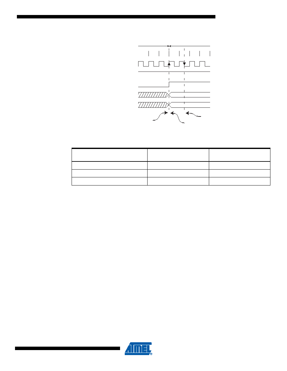
Figure 22-7. ADC Timing Diagram, Free Running Conversion
22.6
Changing Channel or Reference Selection
The MUXn and REFS1:0 bits in the ADMUX Register are single buffered through a temporary
register to which the CPU has random access. This ensures that the channels and reference
selection only takes place at a safe point during the conversion. The channel and reference
selection is continuously updated until a conversion is started. Once the conversion starts, the
channel and reference selection is locked to ensure a sufficient sampling time for the ADC. Con-
tinuous updating resumes in the last ADC clock cycle before the conversion completes (ADIF in
ADCSRA is set). Note that the conversion starts on the following rising ADC clock edge after
ADSC is written. The user is thus advised not to write new channel or reference selection values
to ADMUX until one ADC clock cycle after ADSC is written.
If Auto Triggering is used, the exact time of the triggering event can be indeterministic. Special
care must be taken when updating the ADMUX Register, in order to control which conversion
will be affected by the new settings.
If both ADATE and ADEN is written to one, an interrupt event can occur at any time. If the
ADMUX Register is changed in this period, the user cannot tell if the next conversion is based
on the old or the new settings. ADMUX can be safely updated in the following ways:
a.
When ADATE or ADEN is cleared.
b.
During conversion, minimum one ADC clock cycle after the trigger event.
c.
After a conversion, before the Interrupt Flag used as trigger source is cleared.
When updating ADMUX in one of these conditions, the new settings will affect the next ADC
conversion.
Table 22-1.
ADC Conversion Time
Condition
Sample & Hold (Cycles from
Start of Conversion)
Conversion Time (Cycles)
First conversion
13.5
25
Normal conversions, single ended
1.5
13
Auto Triggered conversions
2
13.5
11
12
13
Sign and MSB of Result
LSB of Result
ADC Clock
ADSC
ADIF
ADCH
ADCL
Cycle Number
12
One Conversion
Next Conversion
34
Conversion
Complete
Sample & Hold
MUX and REFS
Update
发布紧急采购,3分钟左右您将得到回复。
相关PDF资料
PIC16C716-20I/P
IC MCU OTP 2KX14 A/D PWM 18DIP
PIC18F26K80-I/SO
MCU PIC 64KB FLASH 28SOIC
PIC18F26J13-I/SS
IC PIC MCU 64KB FLASH 28SSOP
SFW27R-1STE1
SFW27R-1STE1-FFC/FPC CONN
PIC18F66J15-I/PT
IC PIC MCU FLASH 48KX16 64TQFP
PIC24FV32KA302-I/SO
MCU 32KB FLASH 2KB RAM 28-SOIC
PIC24HJ64GP204-I/ML
IC PIC MCU FLASH 64K 44-QFN
SFW27R-2STE1
SFW27R-2STE1-FFC/FPC CONN
相关代理商/技术参数
PIC16F916-I/SO
功能描述:8位微控制器 -MCU 14KB FL 352R 25 I/O RoHS:否 制造商:Silicon Labs 核心:8051 处理器系列:C8051F39x 数据总线宽度:8 bit 最大时钟频率:50 MHz 程序存储器大小:16 KB 数据 RAM 大小:1 KB 片上 ADC:Yes 工作电源电压:1.8 V to 3.6 V 工作温度范围:- 40 C to + 105 C 封装 / 箱体:QFN-20 安装风格:SMD/SMT
PIC16F916-I/SO
制造商:Microchip Technology Inc 功能描述:8 Bit Microcontroller Clock Speed:20MHz
PIC16F916-I/SOG
制造商:Microchip Technology Inc 功能描述:8BIT MCU FLASH SMD 16F916 SOIC28
PIC16F916-I/SP
功能描述:8位微控制器 -MCU 14KB FL 352R 25 I/O RoHS:否 制造商:Silicon Labs 核心:8051 处理器系列:C8051F39x 数据总线宽度:8 bit 最大时钟频率:50 MHz 程序存储器大小:16 KB 数据 RAM 大小:1 KB 片上 ADC:Yes 工作电源电压:1.8 V to 3.6 V 工作温度范围:- 40 C to + 105 C 封装 / 箱体:QFN-20 安装风格:SMD/SMT
PIC16F916-I/SP
制造商:Microchip Technology Inc 功能描述:8 Bit Microcontroller Clock Speed:20MHz
PIC16F916-I/SS
功能描述:8位微控制器 -MCU 14KB FL 352R 25 I/O RoHS:否 制造商:Silicon Labs 核心:8051 处理器系列:C8051F39x 数据总线宽度:8 bit 最大时钟频率:50 MHz 程序存储器大小:16 KB 数据 RAM 大小:1 KB 片上 ADC:Yes 工作电源电压:1.8 V to 3.6 V 工作温度范围:- 40 C to + 105 C 封装 / 箱体:QFN-20 安装风格:SMD/SMT
PIC16F916-I/SS
制造商:Microchip Technology Inc 功能描述:8-Bit Microcontroller IC
PIC16F916T-E/MLC02
制造商:Microchip Technology Inc 功能描述: